An in-depth guide to how Noiseless InGaAs APDs extract the signal from the noise
24th June 2024
Optical systems operating at infrared wavelengths have become a crucial tool for pinpointing the position of distant objects and are increasingly being sought after for emerging robotics applications that require an accurate 3D view of their surroundings. These time-of-flight systems work by beaming laser light into their environs, and then detecting and analysing the signals that are reflected. Determining the precise location of each object demands a high signal-to-noise ratio, which in practice requires a combination of high laser powers and extremely sensitive detectors.
Infrared systems offer a key advantage here since much higher laser powers can be emitted into the outside world while still operating within the eye-safe regime. However, the limited sensitivity of photodetectors at infrared wavelengths poses a challenge for building high-performance systems in a compact and affordable package. That's because costly and cumbersome fibre lasers must be used to generate enough optical power for the sensors to detect the returning signals, which is not a viable option for mass-market applications.
Phlux Technology has addressed this issue by engineering an infrared sensor that is 12 times more sensitive than its nearest rival. Such enhanced sensitivity allows an optical time-of-flight system to operate with a much cheaper solid-state laser, massively reducing its size, cost and complexity while still being able to visualize the outside world with precision and clarity. Depending on the needs of the application, the enhanced sensitivity can also be harnessed to boost the speed of the system, enable operation at higher temperatures, or to increase the measurement range by as much as 50%.
Detector engineering
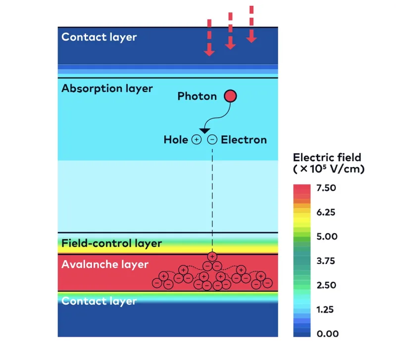
The sensor developed by Phlux is a reimagined version of an avalanche photodiode (APD), a device structure that is widely used to detect weak optical signals. As with any photodiode, an APD exploits a layer of semiconducting material to convert light into an electrical signal. This semiconductor layer absorbs the energy of an incoming photon, releasing an electron-hole pair from the material that can be separated and guided to opposite electrodes with an electric field. To work at infrared frequencies the absorbing material must be made from a compound semiconductor, with the most efficient response provided by indium gallium arsenide (InGaAs).
To detect low photon counts an APD also includes an additional layer to amplify the small photocurrent generated in the absorbing material. In this multiplication layer an extremely strong electric field is used to accelerate the free electrons, causing them to collide with the material's crystal lattice and release more charge carriers into the material. This instigates an avalanche process in which increasing numbers of charge carriers cause more impact ionizations, delivering the gain that allows the signal to be detected by subsequent electronics.
The avalanche diode internal gain mechanism
However, in conventional APDs this avalanche process produces a lot of noise, which compromises the sensitivity that can be achieved. The key problem is that the materials used for the multiplication layer are just as likely to produce holes as electrons from the impact ionizations, with the strong electric field causing the positively charged holes to accelerate in the opposite direction to the negatively charged electrons. This creates a chaotic process that can yield vastly different outcomes each time an electron is injected into the multiplication layer: in some cases, the avalanche process might continue indefinitely, but in others, minimal gain might be achieved. As a result of this random behaviour, noise starts to dominate the response at avalanche gains beyond around 10–20.
In contrast, the multiplication layer in the APD engineered by Phlux is composed of a semiconducting alloy that contains some antinomy. In this novel material, nearly all the impact ionizations produce electrons, and the avalanche process is also restricted to a precise location within the multiplication layer. This almost deterministic process dramatically reduces the excess noise in the system, allowing the device to be operated at avalanche gains of up to 120.
While other attempts have been made to achieve this near-deterministic operation, they have relied on complex device engineering – typically requiring repeating sequences of atomically-thin layers to be grown on top of each other – that has prevented the development of a commercially viable solution. In the Phlux device, however, the alloy used for the multiplication layer is a homogeneous material that enables the use of standard manufacturing processes.
Other factors contribute to the overall sensitivity of the device, with the Phlux engineers paying particular attention to the challenge of reducing the dark current – the baseline noise that results from thermally-generated charge carriers. By optimizing the process parameters, the device design, and the purity of the materials, the dark current in the latest version of the device, branded the Aura Noiseless InGaAs APD, has been reduced by more than 75%.
Reducing excess noise from dark current is the critical factor for improving APD sensitivity.
This unique combination of low excess noise and low dark current has yielded a commercial APD that is 12 times more sensitive than current best-in-class devices, opening new opportunities for engineering cost-effective and compact time-of-flight systems that also consume less power. What's more, the unique design of the Aura device delivers the stability, performance and robustness to enable it to be deployed in a range of real-world scenarios.
Engineered for the real world
For a start, the low noise levels in the Aura APD helps to stabilize the gain provided by the device. One key issue for conventional APDs is that they must be operated close to their breakdown voltage to optimize the gain, but they are difficult to control in this regime because small ripples in the supply voltage can produce large variations in the output. In contrast, Aura APDs can be operated further from the breakdown point, which makes them easier to integrate into a system design.
The Aura devices are also much more resilient to variations in temperature, which is another major problem for APDs that are operated close to breakdown. That's because the breakdown voltage is highly dependent on temperature, with even small changes altering the point of breakdown by hundreds of millivolts. Once the device is integrated into a system, it is also difficult to measure the operating temperature or to modify the supply voltage, which means that specialised electronics must be used to compensate for temperature changes and maintain a constant gain.
Operating the Aura device further from breakdown mitigates against this issue. More significantly, the APD has been engineered to reduce the temperature drift of the breakdown voltage to around 20 mV per Kelvin, up to 10 times lower than other APDs on the market. Meanwhile, the low dark current and excess noise levels also offer integrators the option of operating the device over a wider temperature range without the need for complex thermal management systems.
One of the biggest challenges for optical time-of-flight applications is that the APD must be capable of detecting and handling a wide range of reflected signals. In the case of autonomous driving, for example, the strong laser emission could be bounced back from a black tyre in the distance – requiring high sensitivity to record such low photon counts – or from a highly reflective numberplate positioned right in front of the detector. To survive such extreme powers the APD must have a high damage threshold, with tests showing that the Aura device can still function after being illuminated with repeated infrared laser pulses at powers as high as 40 MW/cm2.
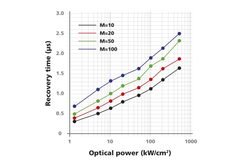
Exposure to high optical powers can also increase the time the device takes to recover from saturation, reducing its ability to respond to the next incoming signal. Speeding up the recovery time is best achieved by matching the output from the APD to the other critical component in the receiver unit, a transimpedance amplifier (TIA), which converts the electrical current generated by the APD into a voltage. To demonstrate this capability, Phlux has engineered a prototype receiver module that, when operating at a gain of 10, offers an overload recovery time of below 1.5 µs after being exposed to a signal with an optical power of 500 kW/cm2 and a recovery time of 2.5 µs when operating at a gain of 100 at 500 kW/cm2.
A shorter recovery time means improved ability to respond to the next incoming signal
Co-designing the APD and TIA also makes is easier to pinpoint the arrival time of each incoming signal, which in turn improves the precision of the distance measurements. Accurate timing requires the signal response to have a rapid rise time and an equally fast decay time, with the prototype module demonstrated by Phlux can distinguish between pulses arriving just 10 ns apart.
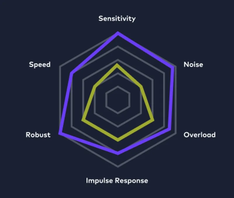
Summary of performance improvements offered by Aura APDs over standard InGaAs devices (not to scale).
By combining unprecedented sensitivity and low noise with optimized performance across all key device parameters - speed, impulse response, overload recovery, and robustness even at high temperatures - the Aura APD can be operated to meet the demands of many different applications. It is also available as a commercial product that can be used as a drop-in replacement for other APDs, allowing system integrators to derive immediate benefit from its breakthrough capabilities.
To find out how the Aura APD could help in your application, get in touch
with the team.